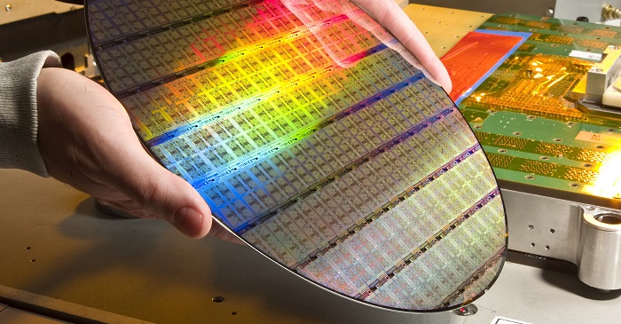
The other name for silicon wafers is substrates. They are a part of electronics and can be understood as thin slices of highly pure crystalline silicon. It is c-Si and is used to produce integrated circuits, a composite of different electronic components.
The semiconductor industry acknowledges the role of patterned silicon wafers as they play a major role in micromechanical devices and electronics. Let’s learn more about these wafers.
Understanding Silicon Wafers
Si Wafers are a big ingredient for microelectronic devices and are useful for building electronic circuits. The main reasons for using them are their affordability and conductivity. The commonness list gets silicon in the 7th place, the 2nd most common element on earth.
There are other elements like beach sand, agate, and others like flint. Further, silicon sees other elements in use in construction materials and buildings, like cement and glass. Also, its need as a semiconductor is high, which also helps its use in the technology and electronic sector.
Usually, these crystals look metallic but do not completely belong to the metals category. They have free electrons as they can move easily between atoms. The other dependable features are that they are good conductors of electricity and support the proper movement of electrons. However, if you look at pure silicon crystal, it works as an insulator and allows very little degree of electricity to pass through it. But, if you want to change it, you must begin doping.
Making Of Silicon Wafers
Did you know that silicon is extracted from sand?
It can come as a surprise to you, but this is true that the purification is done later on. The creation and purification process begins with the heating stage, which continues until the silicon melts and converts into a high-purity liquid. The purity levels likely to be reached are at 99.9999999% purity and, sometimes, even high. Also, there are no defects in it.
After the burning is done, the solidification step comes into the picture. The melted silicon is then converted into a silicon rod or ingot. The solidification is done with the help of fabrication methods, including the Floating Zone and the Czochralski process. The Czochralski process includes placing and using small solid silicons in a pool containing molten silicon.
The particles are pulled together slowly through rotation. The process helps transform the liquid into a cylindrical ingot. Now, that’s why the wafers are available as discs. The ingot develops the pyramidal ends. Right before the cooling stage comes completely, these ends are yanked off.
Usually, the sharp diamond saw blades are used for slicing the product, and that’s how the thin wafers are achieved. Also, it helps in ensuring the same degree of thickness for all wafers.
Types Of Silicon Wafers
The silicon wafers have many things to offer, so they offer different variations. The variations help to serve different needs and purposes, so the demand for different kinds is high.
So, let’s learn about different types of silicon wafers. In the present scenario, there are two varieties of silicon wafers. They are as follows:
1. Undoped silicon wafers
The other name for this one is Intrinsic or Float Zone (FZ). They do not have any dopants within them. They are a result of strictly pure crystalline silicon. It is an ideal semiconductor and hence, can be used accordingly.
2. Doped silicon wafers
These result from certain impure ones, which are noticed in the formation process. The mixture is combined with boron, and the P-type doped is produced. They have positively charged holes. The wafer has a good quantity of dopant that will help ascertain whether the discovered dopant is degenerated or extrinsic. Degeneration means that dopants are higher. However, extrinsic means that there are moderate dopants.
Industrial-Use Cases of Silicon Wafers
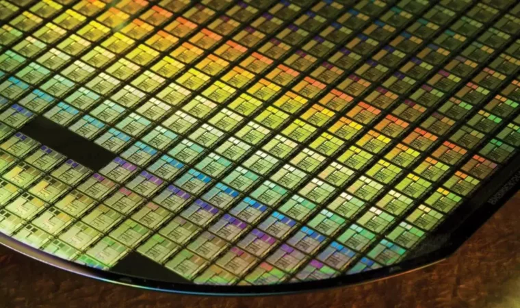
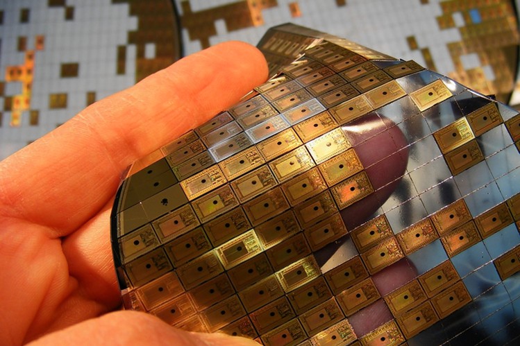
When you explore silicon wafers, you will see that their primary use is Integrated Circuits (ICs) as it forms the critical component. However, as discussed earlier, they are used in different industries and products that are mentioned as follows:
1. Semiconductors
The semiconductors are fabricated, and silicon wafers are used in that process. It helps in adding compactness and efficiency to the final product. They are known for handling a wide degree of current and voltage. Also, they offer a trusted use in optical sensors, lasers, and power devices.
2. Electronics And Computing
The RAM chips are a part of electronics and computing that is indispensable to the new-age technology and era. The RAM chips are somewhat like an IC created with a silicon wafer’s help. Hence, the dependable use makes these present a strong use in this industry.
Further, many manufacturers use them in other electronic devices like automobile electronics, home appliances, smartphones, and drones. Also, if the electronic circuitry device is used anywhere, it uses silicon wafers.
3. Optics
Polished silicon wafers are specially manufactured to be used for optics. They are the perfect pick for reflective optics and Infra-Red.
4. Solar Cells
Silicon wafers are also helpful for solar cells as they add efficiency to the functioning and better sunlight. When the floating zone method fabrication process is used, it helps boost solar cells’ efficiency. The solar cells need to emit purity, and also, there are certain quality levels expected. Hence, silicon wafers are the right pick for the best computing and other electronics delivery.
5. Aerospace Industry
Silicon wafers are known for their superior properties and amazing qualities. They have been a part of this industry even before its concept gained momentum. They are helpful in covering and binding processes of the aerospace industry. Also, it helps shield and insult delicate tools, especially in extreme temperatures. They are the best picks for the functions of this industry.
Conclusion
Silicon wafers have wide usage from everyday things in human life to industries as big as aviation. Also, with leading technology doing rounds in different aspects, silicon wafers are recognized for their potential uses. The development and research will help expand its use to other industries, too.